New Materials Discovery

Novel nanomaterials with tunable electronic, optical, and magnetic properties are vital to emerging applications in energy conversion, quantum information processing, and photonic technologies. Our research focuses on discovering new semiconducting nanomaterials and quantum building blocks through chemical vapor deposition (CVD) and wet-chemical synthesis, with precise control over lattice structure and dimensionality, crystal morphology, and chemical composition. Establishing clear correlations between crystal structure and electronic, optical, and magnetic behavior is essential to enabling their integration into high-performance device architectures.
Yadav, Chemistry of Materials,2023
Yadav, ACS Nano, 2025
Yadav, ACS Materials Au, 2026
Sheng, Advanced Optical Materials, 2024, and more
Unconventional Doping
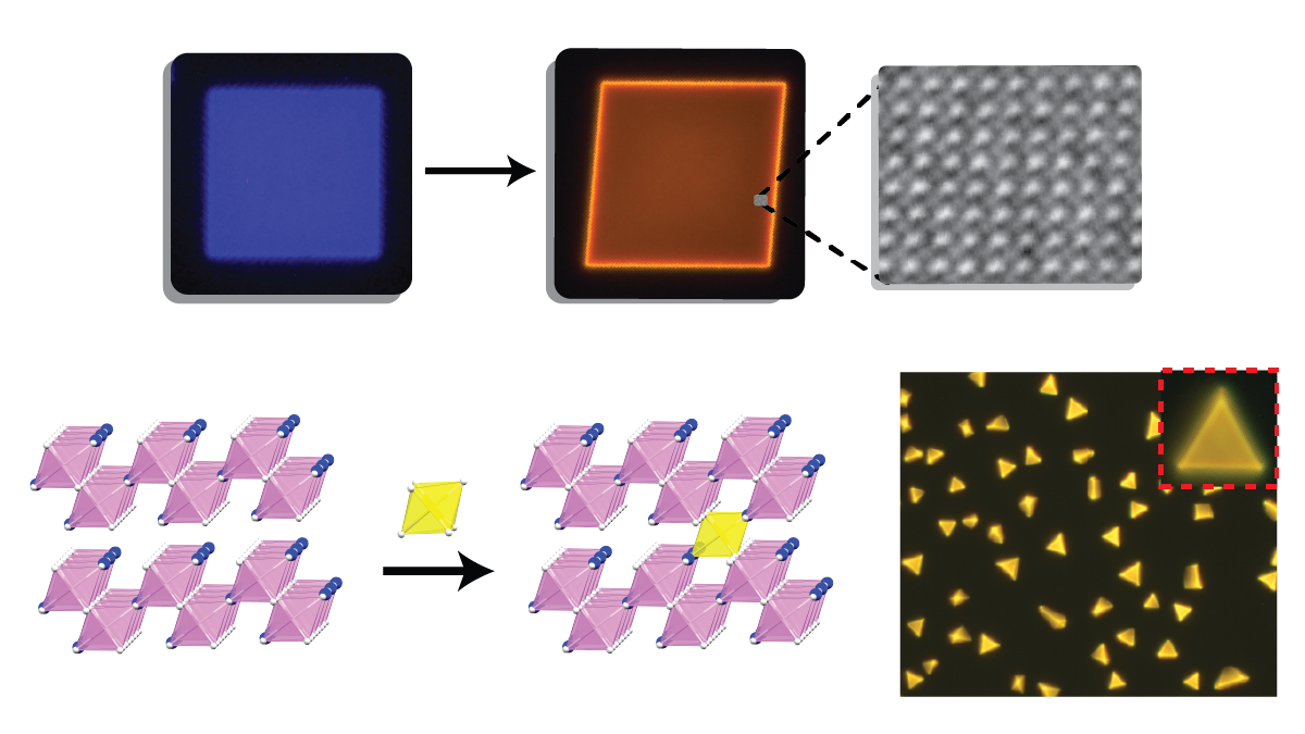
Doping in crystalline solids offers a powerful means to engineer a material’s fundamental properties. Our CVD-based strategies enable new ways to realize non-traditional and non-equilibrium doping configurations and to manipulate the behaviors of charge carriers in semiconducting solids. Through this control, we aim to enhance light–matter interactions for advanced optoelectronic, spintronic, and spin-photonic applications.
Yadav, ACS Nano, 2025
Moon, ACS Nano, 2025
Biswas, Journal of the American Chemical Society, 2024, and more
Optical Metamaterials

The Kim group investigates the meta-photonic behavior of nanoscale metamaterials, with an emphasis on periodically repeated structures that manipulate light at subwavelength scales. Our research focuses on one-dimensional (1D) dielectric optical metawires capable of guiding, confining, orienting, and absorbing light with high precision, enabling device concepts with unprecedented spatial and spectral control.
Sah, Journal of Physical Chemistry C, 2025
Chung, Journal of the American Chemical Society, 2024
Gain, Optics Letters, 2023
Mann, ACS Applied Nano Materials, 2021, and more